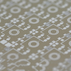
The new technology offered by InSensor™ is the integration between ceramic PZT thick films and various substrates. It was developed using our specialist knowledge on the compatibility between the substrates, the electrodes and the active film. The substrates that we have focused on so far are used in many applications, e.g. the electronics industry:
Silicon
- Used in MEMS applications
Alumina
- A popular and inert substrate in the electronics industry
Porous ceramic
- Used for high-frequency transducers due to the acoustic properties of the material
Thanks to our years of experience with materials and processes, the InSensor™ team may also be able to integrate the PZT thick film technology with other substrates. We will be happy to help you in the development and production of new devices for your applications. Please contact us with details of your specific challenge.
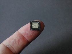
Our InSensor™ piezoelectric thick films can be used in the following applications:
- High-frequency acoustic transducers
- Phased and annular arrays
- MEMS accelerometers
- Energy harvesting
How do you make the InSensor™ material?
InSensor™ uses two methods for deposition of PZT thick film:
- Screen printing
- Pad printing
Screen printing is a well known technology used in the industry to print graphic illustrations, circuitry, surface protection layers etc. The printing equipment for screen printing is readily available at an affordable price and the technology has had time to mature.
Screen printing is well suited for printing on large areas, but unfortunately it is limited to flat substrates. In order to print on surfaces with complex topography (e.g. curved surfaces), InSensor™ has developed a material which can be deposited using pad printing.
Pad printing is also a well known technology often used for printing graphic images on round surfaces such as glass spheres, pens, golf balls etc. The marriage between pad printing and PZT thick film technology is something that has been developed internally in InSensor™ and only we have the capability to offer this solution. Using our pad printing technique we can deposit the active layers on substrates with a radius of curvature down to 10 mm. We can pattern the layers to form complex structures such as linear and annular arrays.
The simplicity and reliability of these manufacturing processes are brought together with an extensive know-how on materials and device design to form a versatile yet strong technology platform.
Here to help you at all stages of development
For products going into the market, the InSensor™ team already has experience with the up-scaling required to go into mass production and will be able to supply high volume.
We assist partners throughout all the phases of development, with technology, during the design stage, with packaging solutions and up-scaling and manufacturing.
Contact us to find out how we can help you.

 EN
EN